In an era of rapid technological advancement, the camera PCB (Printed Circuit Board) industry is demonstrating robust growth momentum.
As demand for cameras continues to surge across sectors such as smartphones, security surveillance, and intelligent vehicles, camera PCBs—as a critical component—are likewise encountering expansive market opportunities. In the smartphone market, high-resolution cameras have become a focal point of competition among major manufacturers, thereby imposing heightened performance requirements on camera PCBs. PCB designs that prioritize thin profiles, high density, and exceptional reliability are better positioned to meet the spatial constraints and performance stability demands of smartphones. Concurrently, to accommodate the ever-evolving external designs of mobile devices, camera PCB technology is undergoing continuous innovation. The application of flexible PCBs, for instance, enables cameras to be installed with greater flexibility within the internal architecture of a phone, unlocking new possibilities for handset design.
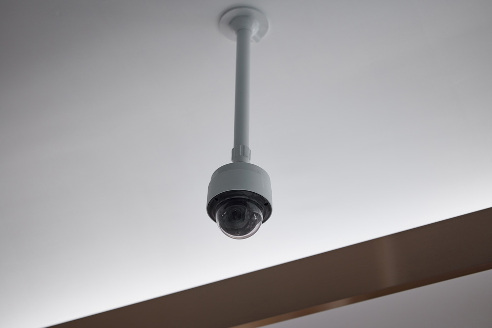
The security surveillance sector similarly serves as a significant driver of camera PCB development. The widespread deployment of high-definition cameras necessitates high-performance PCBs to ensure the stability and clarity of image transmission. Furthermore, with the evolution of intelligent security systems, camera PCBs must not only deliver robust signal transmission performance but also support the execution of intelligent analytic algorithms. For example, advanced security camera PCBs are now capable of enabling functions such as facial recognition and behavioral analysis, providing more sophisticated, intelligence-driven solutions for the security monitoring industry.
In the realm of intelligent vehicles, the role of cameras has become increasingly prominent. Cameras integrated into autonomous driving assistance systems require high-precision PCBs to guarantee accurate image capture and processing. The demanding automotive environment imposes exceptionally stringent reliability requirements on camera PCBs, which must endure the rigors of high temperatures, continuous vibration, and other harsh conditions. Simultaneously, as automotive electronics continue to advance, camera PCBs are trending toward greater integration and miniaturization to satisfy the automotive industry's strict mandates for space efficiency and performance.
To address these market imperatives, enterprises within the camera PCB industry are steadily increasing their R&D investment and actively adopting advanced production technologies and equipment. Techniques such as high-precision laser drilling and fine-line etching are being employed to enhance manufacturing precision and overall PCB performance. At the same time, companies are strengthening collaboration with upstream and downstream partners to jointly propel innovation and development in camera PCB technology.
Nevertheless, the camera PCB industry also confronts a set of challenges. On one hand, fluctuations in raw material prices and increasingly stringent environmental regulations impose certain cost pressures on enterprises. On the other hand, market competition is intense, compelling companies to continually sharpen their core competencies in order to secure a foothold in the marketplace.
Looking ahead, as technological progress persists unabated, the camera PCB industry is poised to maintain its trajectory of rapid expansion. Enterprises will persist in innovating and introducing ever more advanced products, thereby providing robust support for camera applications across a diverse array of fields. Concurrently, the industry will place greater emphasis on environmental stewardship and sustainable development, steering the camera PCB sector toward higher quality and greener manufacturing practices. It is believed that in the near future, the camera PCB industry will continue to deliver new levels of convenience and delightful surprises to our daily lives.